


A New Dawn in Solar Energy: The Promise of Perovskite
By Neha Bisht
On a warm morning, as sunlight spills across rooftops and fields, it’s easy to forget that this endless light could power our entire world. For centuries, humans have relied on fire, coal, oil, and gas to keep their lives running – but all of these come at a cost. Rising temperatures, melting glaciers, and polluted air remind us that it’s time for a change. And that change may come from something as simple – and as brilliant – as the Sun.
Solar energy is one of the cleanest and most abundant forms of energy on Earth. Every hour, the Sun gives off more energy than the world consumes in an entire year. By harnessing just a fraction of it, we can reduce our dependence on fossil fuels, lower our electricity bills, and protect the planet.
How Solar Cells Work
Traditional solar panels are mostly made from silicon, a stable material that converts sunlight into electricity. When sunlight hits the panel, it energizes tiny particles called electrons, making them move and create an electric current. Generally, a single solar cell is a tiny unit that generates electricity, while a solar panel is made up of many such cells connected together to produce more power.
Silicon solar panels – those familiar blue-black sheets we see on rooftops – have powered the solar revolution for decades. They are reliable and efficient – but making them requires high temperatures, heavy equipment, and significant
cost. As well, they can’t easily adapt to new uses like flexible surfaces or window coatings. Researchers have long been searching for new materials that are cheaper, lighter, and even more efficient. And that’s where perovskite comes in.
The Rise of Perovskite Solar Cells Perovskite is not a single material but a family of compounds that share a unique crystal structure – named after a mineral first discovered in Russia. Scientists found that this structure can absorb sunlight exceptionally well, making it ideal for solar applications.
Since their first appearance in 2009, perovskite solar cells have taken the scientific world by storm. Their efficiency in converting sunlight to electricity has skyrocketed from less than 4% to over 26% – a remarkable leap achieved in just over a decade.
Even more impressively, these cells can be manufactured using simple, low-cost methods – such as solution coating or inkjet printing and can be applied to a variety of surfaces including glass, plastic, and metal. The perovskite solution can even be deposited on flexible substrates, making it possible to create lightweight and bendable solar devices. This innovation opens the door to a future where solar panels are no longer limited to rigid rooftop installations – they could be painted onto walls, coated on windows, or even printed like newspapers.
“Since their flrst appearance in 2009, perovskite solar cells have taken the scientiflc world by storm.”
Challenges on the Horizon
Despite their incredible promise, perovskite solar cells still face some challenges before they can become a part of our everyday lives. The materials used are quite sensitive to moisture, heat, and sunlight, which can make them less stable over time. In addition, many high-efficiency perovskites still contain toxic lead, which poses environmental concerns.
However, scientists across the world are working tirelessly to overcome these issues – by developing new materials, protective layers, and smarter device designs that can make these solar cells more durable and safer to use.
In my research, I focus on improving the stability of perovskite solar cells, particularly using the n–i–p type device structure. You can imagine this structure as a delicate layered sandwich, where each layer plays an important role in converting sunlight into electricity.
At the very front on a glass substrate is a thin transparent layer called FTO (fluorine-doped tin oxide) which acts like a window that lets sunlight in while conducting electricity. Next to it lies the n-type layer, known as the electron transport layer (ETL), which collects the negatively charged particles (electrons) produced when sunlight hits the cell. Next comes the i-type perovskite layer, the heart of the device, where sunlight is actually absorbed and turned into electrical energy. Beneath that lies the p-type layer, or hole transport layer (HTL), which carries the positive charges. Finally, a thin metal electrode – usually made of gold or silver – is added on top to collect the electric current and complete the circuit (see the schematic of this “sandwich” structure).
In my experiments, I use materials like titanium dioxide (TiO2) or tin oxide (SnO2) for the electron transport layer, formamidinium lead triiodide (FAPbI3) as the light-absorbing layer, and Spiro-OMeTAD for the hole transport layer. All these layers are deposited using a process called spin coating, where a small amount of liquid solution is dropped onto a surface and spun at high speed to form a thin, even film – much like spreading batter evenly on a frying pan. Achieving uniform thickness and smooth surfaces is crucial for getting good performance (high efficiency). Finally, a thin layer of gold is deposited as the top electrode using a thermal evaporator system.
After preparing the layers, I analyze each one to study its crystal structure, surface texture, and optical properties, ensuring that the films are well-formed and ready for device fabrication. Once the complete solar cell is made, I test its performance using a solar simulator, which mimics real sunlight in the lab. The device’s behavior is recorded on a graph called the J–V curve, from which I calculate key parameters such as current (JSC), voltage (VOC), fill factor (FF), and power conversion efficiency (PCE) – all of which reveal how efficiently the device converts sunlight into electricity.
Other measurements – like external quantum efficiency (EQE) and dark J–V measurement help me understand how charges move through the device and what might be limiting its performance.
To enhance the long-term performance and stability of my devices, I use a technique called additive engineering, where small chemical additives are mixed into the FAPbI3 perovskite layer. These additives help improve crystal growth, film quality, and resistance to environmental damage, making the solar cells more reliable and durable (see photograph).
Device fabrication requires continuous and precise work, so there are days when I spend up to 14 hours in the lab, carefully completing each step without interruption. At times, I work day and night to complete a fabrication process and ensure that every layer and measurement is done perfectly. Tedious work, yes, but it carries promise for the future.
“The Sun shines for everyone – and with perovskite solar cells, we are learning how to truly embrace its light.”
A Brighter, Greener Tomorrow
Imagine a world where your building windows generate power during the day, or where your backpack charges your phone as you walk. With continued research and innovation, perovskite solar cells could turn this vision into reality.
The journey toward clean energy is not just about technology – it’s about hope, responsibility, and imagination. Each solar panel installed, each watt of sunlight converted, brings us closer to a future where energy is clean, affordable, and shared by all.
The Sun shines for everyone – and with perovskite solar cells, we are learning how to truly embrace its light.
The Author
A native of India, Neha Bisht is pursuing her PhD research at Chonnam National University’s School of Materials Science and Engineering. She loves to meet new people and make new friends. Neha endeavors to contribute to the well-being of society in whatever way she can. Follow @philla_korea
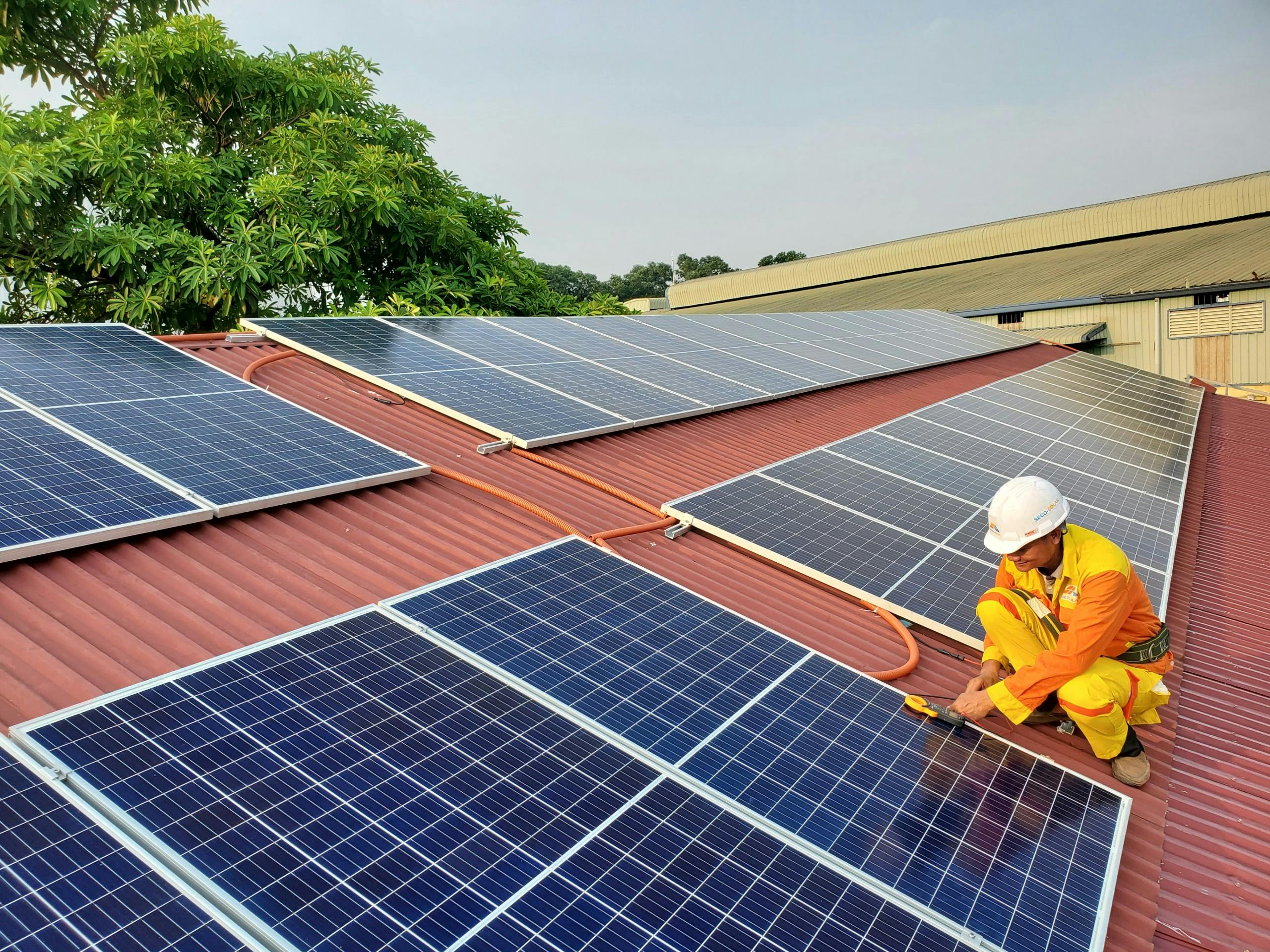
Cover Photo: Commercial silicone solar panels on a rooftop. (Trinh Trần)